While chips have become ubiquitous, Moore’s Law has remained a self-fulfilling prophecy even half a century later. Not bad for an industry where the time scale is not measured in decades and centuries, but in annual quarters, says Shivanand Kanavi.
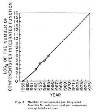
‘The complexity [of integrated circuits] for minimum costs has increased at a rate of roughly a factor of two per year. -- Gordon E Moore, Electronics, VOL 38, NO 8, 1965
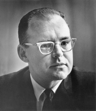
This year marks 50 years of the reign of Moore's Law. Gordon Moore, the co-founder of Intel, made a prediction in 1965 that the number of transistors on a chip and the raw computing power of microchips would double every year while the cost of production would remain the same.
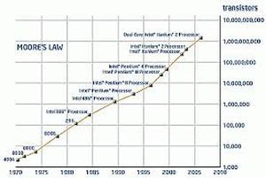
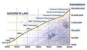
When he made this prediction, chips had only 50 transistors; today, a chip can have more than four billion transistors. Thus, the power of the chip has increased by a factor of 80 million in about 38 years!
The only correction to Moore’s Law is that nowadays the doubling occurs every 18 months, instead of a year. As for cost, when transistors were commercialised in the early 1950s, one of them used to be sold for $49.95; in 2015 a chip like the 18 Core Xeon Haswel EP, which has 5.5 billion transistors, costs about $4,000. In other words, the cost per transistor has dropped by a factor of 70 million.
 This is what has made chips affordable for all kinds of applications: Personal computers that can do millions of arithmetic sums in a second, telecom networks that carry billions of calls, and Internet routers that serve up terabytes of data (a tera byte is a thousand billion byte).
The reduced costs allow chips to be used in a wide range of modern products. They control cars, microwave ovens, washing machines, cell phones, television sets, machine tools, wrist-watches, radios, audio systems and even toys.
In the not too distant future, the Government of India may consider the idea of providing a billion Indians with a chip-embedded Aadhar card carrying all personal data needed for public purposes. Already credit cards, debit cards, driving licences etc in India carry chips.
According to the US Semiconductor Industry Association, the industry produces a billion transistors per year for every person on earth (seven billion inhabitants)! The global semiconductor industry is estimated to be a $300 billion-a-year business. Electronics, a technology that was born at the beginning of the 20th century with the discovery of the electron, has today been integrated into everything imaginable.
 The Nobel Committee paid the highest tribute to this phenomenal innovation in 2000 when it awarded the Nobel Prize in Physics to Jack Kilby who invented the integrated circuit, or the chip, at Texas Instruments in 1958. Considering the breathtaking advances in the power of chips and the equally astonishing reduction in their cost, people sometimes wonder whether this trend will continue forever. Or will the growth come to an end soon and the so-called Moore's Law cease to be valid?
The Institute of Electrical and Electronics Engineers, or (IEEE as ‘I-triple E’) -- the world’s most prestigious and largest professional association of electrical, electronics and computer engineers -- conducted a survey among 565 of its distinguished fellows, all highly respected technologists.
One of the questions the experts were asked was: How long will the semiconductor industry see exponential growth, or follow Moore’s Law? The results of the survey, published in the January 2003 issue of IEEE Spectrum magazine, saw the respondents deeply divided.
An optimistic 17 per cent said more than 10 years, a majority-- 52 per cent -- said five to 10 years and a pessimistic 30 per cent said less than five years. More than 10 years after the survey, the law still seems to be going strong.
Printing technology and chip-making
The chip-making process, in its essence, resembles the screen-printing process used in the textile industry. When you have a complicated, multi-coloured design to be printed on a fabric, the screen printer takes a picture of the original, transfers it to different silk screens by a photographic process, and then uses each screen as a stencil, while the dye is rolled over the screen. One screen is used for each colour. The only difference is in the size of the design.
 With dress material, print sizes run into square metres; with chips, containing millions of transistors (the 6 core i7, for example, has 1.2 billion transistors), each transistor occupies barely a square micron.
How is such miniature design achieved?
There are all kinds of superfine works of art, including calligraphy of a few words on a grain of rice. But the same grain of rice can accommodate a complicated circuit containing about 3,000 transistors!
How do chipmakers pull off something so incredible?
In a way, the chip etcher’s approach is not too different from that of the calligraphist writing on a grain of rice. While the super-skilled calligraphist uses an ordinary watchmaker’s eyepiece as a magnifying glass, the chipmaker uses very short wavelength light (ultraviolet light) and sophisticated optics to reduce the detailed circuit diagrams to a thousandth of their size.
These films are used to create stencils (masks) made of materials that are opaque to light. The masks are then used to cast shadows on photosensitive coatings on the silicon wafer, using further miniaturisation with the help of laser light, electron beams and ultra-sophisticated optics to imprint the circuit pattern on the wafer.
The process is similar to the good old printing technology called lithography, where the negative image of a text or graphic is transferred to a plate covered with photosensitive material, which is then coated by ink that is transferred to paper pressed against the plates by rollers. This explains why the process of printing a circuit on silicon is called photolithography.
Of course, we are greatly simplifying the chip-making methodology for the sake of explaining the main ideas. In actual fact, several layers of materials -- semiconductors and metals -- have to be overlaid on each other, with appropriate insulation separating them.
Chipmakers use several sets of masks, just as newspaper or textile printers use different screens to imprint different colours in varied patterns. While ordinary printing transfers flat images on paper or fabric, chipmakers create three dimensional structures of micro hills and vales by using a host of chemicals for etching the surface of the silicon wafer.
The fineness of this process is measured by how thin a channel you can etch on silicon. So, when someone tells you about 45 nanometre (nanometre is one millionth of a milli metre) technology being used by leading chipmakers, they are referring to hi-tech scalpels that can etch channels as thin as 45 nanometres. To get a sense of proportion, that is equivalent to etching over 2,000 parallel ridges and vales on the diameter of a single strand of human hair!
In 2010 most fabs used 45 nanometre technology; in 2015 many leading fabs have commercialised 22 nanometre technology and are experimenting with 14 nanometre technology in their labs.
What does this mean? Well, roughly each new technology is able to etch a transistor in half the surface area of the silicon wafer than the previous one. Lo and behold, the ‘secret’ of Moore’s Law of doubling transistor density on a chip!
Why Moore's Law must end
What are the problems in continuing this process? Making the scalpels sharper is one. Sharper scalpels mean using shorter and shorter wavelengths of light for etching. But, as the wavelength shortens we reach the X-ray band, and we do not yet have X-ray lasers or optics of good quality in that region.
There is another hurdle. As circuit designs get more complex and etching gets thinner, the masks too become thinner. A law in optics says that if the dimensions of the channels in a mask are of the order of the wavelength of light, then, instead of casting clear shadows, the masks will start ‘diffracting’ -- bands of bright and dark regions would be created around the edges of the shadow, thereby limiting the production of sharply defined circuits.
Moreover, as the channels get thinner there are greater chances of electrons from one channel crossing over to the other due to defects, leading to a large number of chips failing at the manufacturing stage.
Surprisingly, though, ingenious engineers have overcome the hurdles and come up with solutions that have resulted in further miniaturisation.
At every stage, engineers have had to fine-tune various elements of the manufacturing process and the chips themselves. For example, in the late 1970s, when memory chipmakers faced the problem of limited availability of surface, they found an innovative answer to the problem.
“The dilemma was,” says Pallab Chatterjee, “should we build skyscrapers or should we dig underground into the substrate and build basements and subways?” While working at Texas Instruments in the 1970s and 1980s, Chatterjee played a major role in developing reliable micro transistors and developing the ‘trenching’ technology for packing more and more of them per square centimetre. This deep sub-micron technology resulted in the capacity of memory chips leapfrogging.
Another person of Indian origin, Tom Kailath, an emeritus professor of communication engineering and information theory at Stanford University in the US, developed signal processing techniques to compensate for the diffractive effects of masks.
A start-up founded by him successfully commercialised Kailath’s ideas. Kailath’s contribution was an instance of the cross-fertilisation of technologies, with ideas from one field being applied to solve problems in a totally different field. Well known as a leading academic and teacher, Kailath takes great satisfaction in seeing some of his highly mathematical ideas getting commercialised in a manufacturing environment.
Another leading researcher in semiconductor technology who has contributed to improving efficiencies is Krishna Saraswat, also at Stanford University.
“When we were faced with intense competition from Japanese chipmakers in the 1980s, the Defence Advanced Research Projects Agency, DARPA, a leading financer of hi-tech projects in the US, undertook an initiative to improve fabrication efficiencies in the American semiconductor industry,” says Pallab Chatterjee. “We at Texas Instruments collaborated with Saraswat at Stanford, and the team solved the problems of efficient batch processing of silicon wafers.”
One of the ways diligent Japanese companies became more efficient than the Americans was by paying attention to ‘clean-room’ conditions. Pallab Chatterjee and Krishna Saraswat spotted it and brought about changes in manufacturing techniques that made the whole US chip industry competitive.
The devil is in the interconnects!
One of Krishna Saraswat’s main concerns today is to reduce the time taken by signals to travel between chips and even within chips. “The ‘interconnects’ between chips can become the limiting factor to chip speeds, even before problems are faced at the nano-physics level,” he explains.
Clearly, semiconductors have broken barriers of all sorts. With their low price, micro size and low power consumption, they have proved to be wonder materials.

Did India miss the electronics bus? Yes, it certainly did during 1970 and 2000. There is the apocryphal story of Robert Noyce coming to Delhi and staying for two weeks in 1969-70 trying to convince the Government of India that they should let Intel build a chip fab here. Not surprisingly, he was turned away!
However, later developments in chip design technology have allowed for fabrication and design to be separated. It is notable that technologists of Indian origin like Suhas Patil, Prabhu Goel, Raj Singh, Rajiv Madhavan, Prakash Bhalerao have contributed to this separation of VLSI (Very Large Scale Integrated Circuits) design software from chip fabrication.
Now cutting edge chips are being designed for the world in Bengaluru, Pune and Hyderabad while they may be fabricated in South East Asia, Korea, Taiwan or China. In technological terms if not in business terms, we seem to have caught the electronics bus at the next bus stop, since 80 per cent of the cost of the chip lies in design and testing.
IT industry veterans like F C Kohli are not satisfied with it.Kohli advocated developing appropriate courses in IITs and other engineering colleges to develop the human resources for high end chip design and testing since the 1980s and 1990s.
Kohli emphasises that India needs to produce about 6,000 MTechs (four to five times the current output) every year in VLSI design to reach the sophistication of Israel, which is a leading player in the field.
If a modern-day cell phone were to be made of vacuum tubes instead of micro chips, it would be as tall as the Qutub Minar, and would need a small power plant to run it!
While chips have become ubiquitous, Moore’s Law has remained a self-fulfilling prophecy even 50 years later. Not bad for an industry where the time scale is not measured in decades and centuries, but in annual quarters!
Shivanand Kanavi is a theoretical physicist, senior journalist and author and former vice president, Tata Consultancy Services.





 © 2025 Rediff.com -